MSMP2 - Dual Core OSM SoM
STM32MP2 for Secure and AI Applications

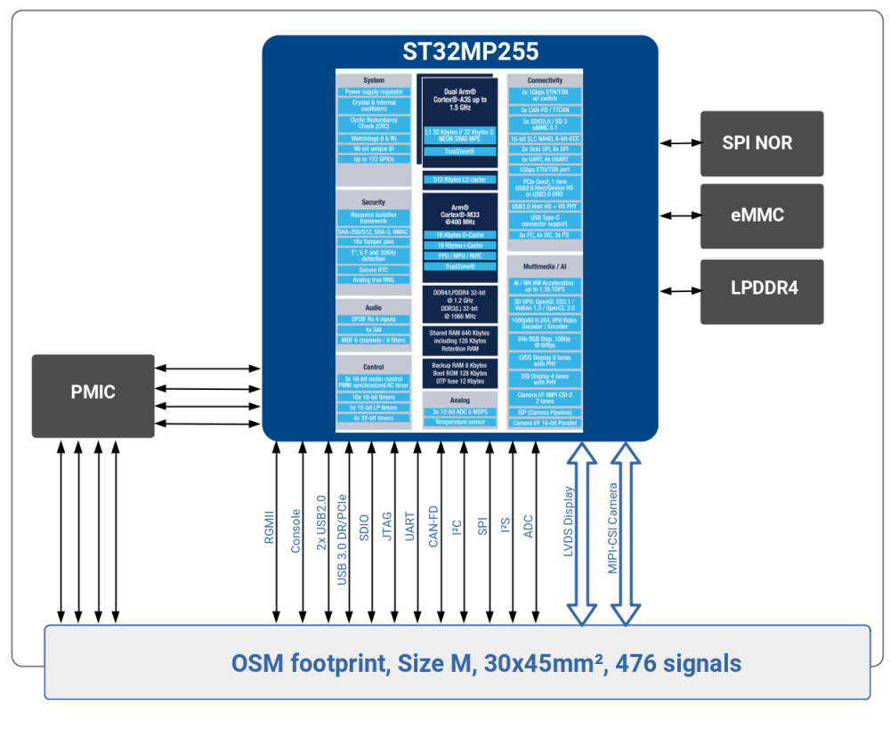
The MSMP2 is the Open Standard Module compliant System-In-Package based on STMicroelectronics STM32MP2 Family architecture offering high-performance dual CortexA35 cores in combination with a CortexM33 core. The MSMP2 combines compact design and a wide range of services, bringing low power consumption, thermal efficiency and low-cost to embedded systems.
The STM32MP2 general-purpose microprocessor units (MPUs) are built around two CortexA7 CPU cores. Peripheral functions include support for multiple interfaces, such as two Gigabit Ethernet interfaces, an USB3.0DRD interface, two USB 2.0 channels, and two CAN channels, as well as A/D converter modules, making it ideal for applications such as HMI devices, industrial control and gateway devices. The chosen OSM form factor supports 476 contacts, offers almost all of the CPU functionality on the contacts and is therefore suitable for most industrial applications.
In addition to a wide range of services, the MSMP2 modules also offer new functionalities in terms of flexibility and processing. The OSM Systems-in-Packages can be individually adapted to the respective customer requirements due to four different form factors.
Features
- Up to 64-bit dual-core Arm® Cortex®-A35, up to 1.5 GHz
- 32-Kbyte I + 32-Kbyte D level 1 cache for each core
- 512-Kbyte unified level 2 cache
- Arm® NEON™ and Arm® TrustZone®
- 32-bit Arm® Cortex®-M33 with FPU/MPU, up to 250 MHz
- L1 16-Kbyte I / 16-Kbyte D
- Arm® TrustZone®
- 32-bit Arm® Cortex®-M0+ in SmartRun domain, up to 200 MHz (up to 16 MHz in autonomous mode)
- Camera interface #1 (5 Mpixels @30 fps)
- MIPI CSI-2®, 2× data lanes up to 2.5 Gbit/s each
- Lite-ISP, demosaicing, downscaling, cropping, 3 pixel pipelines
- Optional 3D GPU: VeriSilicon® - Up to 900 MHz
- OpenGL® ES 3.1 - Vulkan 1.3
- OpenCL™ 3.0, OpenVX™ 1.3
- Up to 150 Mtriangle/s, 900 Mpixel/s
- LCD-TFT controller
- LVDS, 4× data lanes, up to 1.1 Gbit/s per lane
- Up to QXGA (2048 × 1536) @60 fps
- Artificial intelligence
- Optional NPU: VeriSilicon® - Up to 900 MHz
- TensorFlowLite - ONNX - Linux NN
- Video processing
- Optional hardware video encoder and decoder up to 600 MHz
- H264/VP8 up to FHD (1920×1080) @60 fps
- JPEG up to 500 Mpixel/s
- 128 Kbytes of video RAM
- 512MB – 2GB LPDDR4 RAM
- 4GB – 64GB eMMC NAND Flash
- up to 2x Ethernet 100M/1GB
- 2x CAN bus
- 1x USB-2.0 host
- 1x USB-3.0DRD (alternatively 1x PCIe)
- Debug Console
- up to 3x UART
- 2x I2C
- 3x SPI
- I2S
- SD card
- JTAG
- up to 13x ADC
- up to 23x PWM
- GPIO
Block Diagram
Pictures


Order Codes
MSMP255D-BBA
- STM32MP255D
- 1GB LPDDR4 RAM
- 8GB eMMC
- 128MBit SPI NOR
- 0°..+70°C
OSM Standard |
The idea of all Open Standard Modules (OSM) is to create a new, future proof and versatile standard for small-size, low-cost embedded computer modules, combining the following key characteristics:
- different architectures available on the same footprint, scalability in function and performance
- four different mechanical sizes and pin counts, downwards compatible
- pre-defined soft- and hardware interfaces
- specification and design guide publicly available
- design support for baseboard integration, driver development and mass production by ARIES Embedded
- directly assembly to the baseboard without connectors using LGA (Land Grid Array) technology
- completely machine processible during soldering, assembly and testing
The Open Standard Module specification allows developing, producing and distributing embedded modules for the most popular MCU32, ARM and RSICV architectures. For a growing number of IoT applications this standard helps to combine the advantages of modular embedded computing with increasing requirements regarding costs, space and interfaces.